
Projects
Discovery Project
My project files can be found here. This project is still technically a work in progress, but I wanted to share what I have learned and done so far.
Idea
For my Discovery Project for ECE Discovery Studio, I decided to start making a keyboard PCB from scratch. I decided to use MX style switches as they were relatively easy to work with and there are tons of resources online about them. MX switches are some of the more readily available key switches on the market, so I thought it would be easier to find as well. At first, I wanted to add other peripherals such as a rotary encoder or an OLED display, but due to the complexity and time constraints of the project, I was not able to incorporate them into my design. I wanted the keyboard to use USB 2.0 Type C as the Type C connector is becoming more universal. The keyboard layout follows an 83 key layout, essentially a full size keyboard minus the numpad and three keys in the top right cluster. I decided to go with this project because I wanted to learn the basics of PCB design and how to use KiCAD.
I used a couple of tutorials to help me along this project, here are the links: ai03’s Keyboard Guide, Masterzen’s Keyboard Guide, and Noah Kiser’s TKL Keyboard Series. Unfortunately, some of these tutorials were a bit flawed with their fundamentals, leading to a generally messy, albeit informative PCB design experience.
Progress
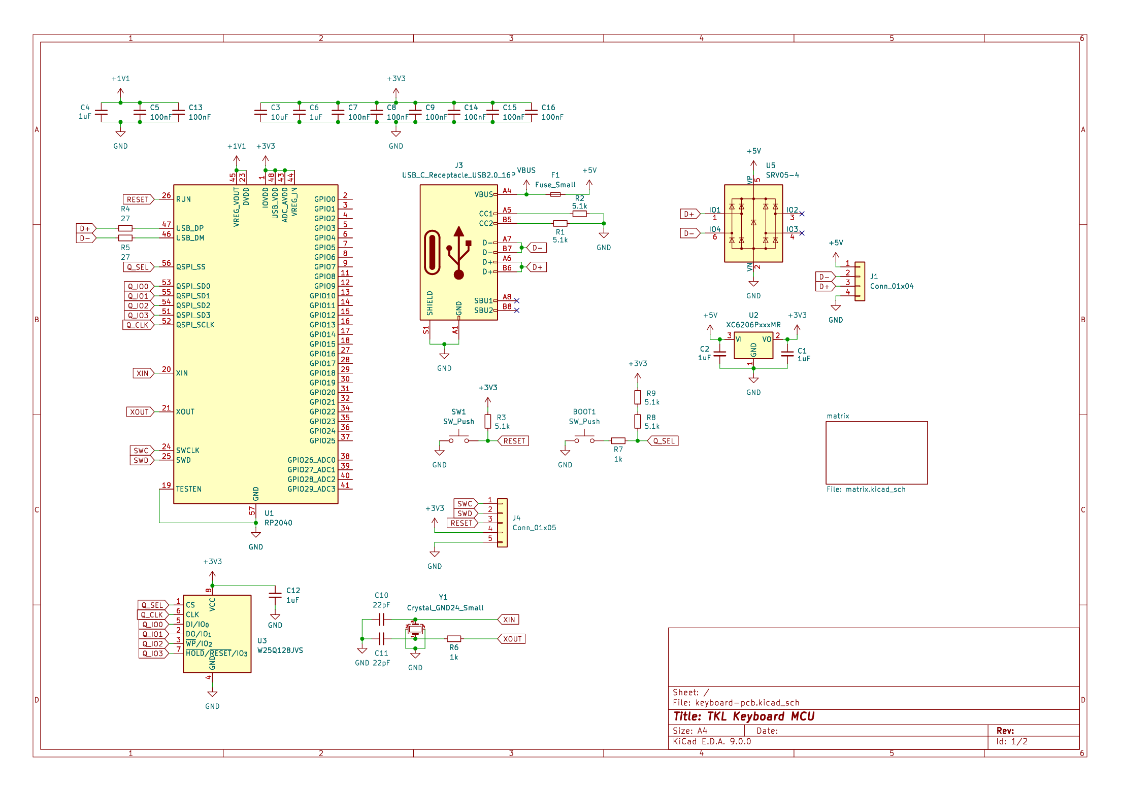
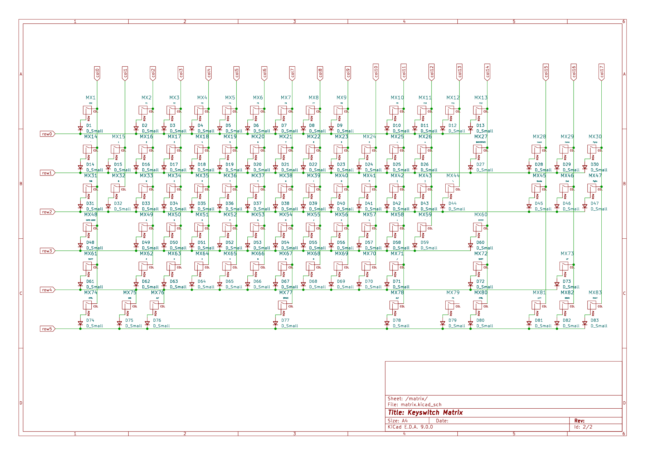
In the first two weeks, I was able to construct a draft schematic of the micro-controller system (picture below). As per the tutorials, the general structure of the schematic held a micro-controller unit, voltage regulator (5V to 3.3V), a reset switch with a 5 pin header as backup, a boot switch that went with a memory chip (for boot purposes), ESD protection, crystal, decoupling capacitors, the USB 2.0 Type C receptacle, and the key switch matrix which involved the MX switches and their respective diodes. The key switch matrix houses all the MX switches and the rows/columns are intentionally labeled to simply IO connections with the motherboard.
Microcontroller:
Switch Matrix:
Through making these peripherals and looking through the tutorials, I was able to learn some KiCAD macros/hotkeys to make designing more efficient. I also learned some basic design rules (e.g. power points up and ground points down) that I can use if I decide to make another PCB in the future. Since nothing is set in stone at the moment, anything about the schematic choices can change.
For the last three weeks leading up to the showcase, I worked on the PCB layout itself. I ended up completing 80% or so of the first draft as I am yet to wire the key switch matrix and plug the respective rows and columns to the micro-controller unit. I was able to complete a rough draft of the USB 2.0 connector portion:
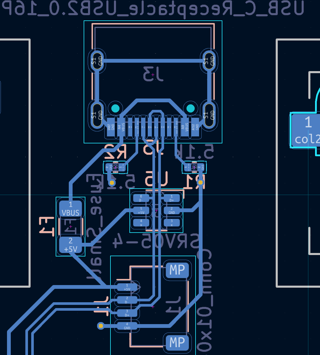
While not perfect (several design flaws yet to fix), there were no errors in the DRC checker. After wiring up the USB connector, I went onto wiring the rest of the smaller components such as the decoupling capacitors, voltage regulator, boot and reset switches, 5-pin header, memory chip, etc. Here is the general structure of the MCU loop:
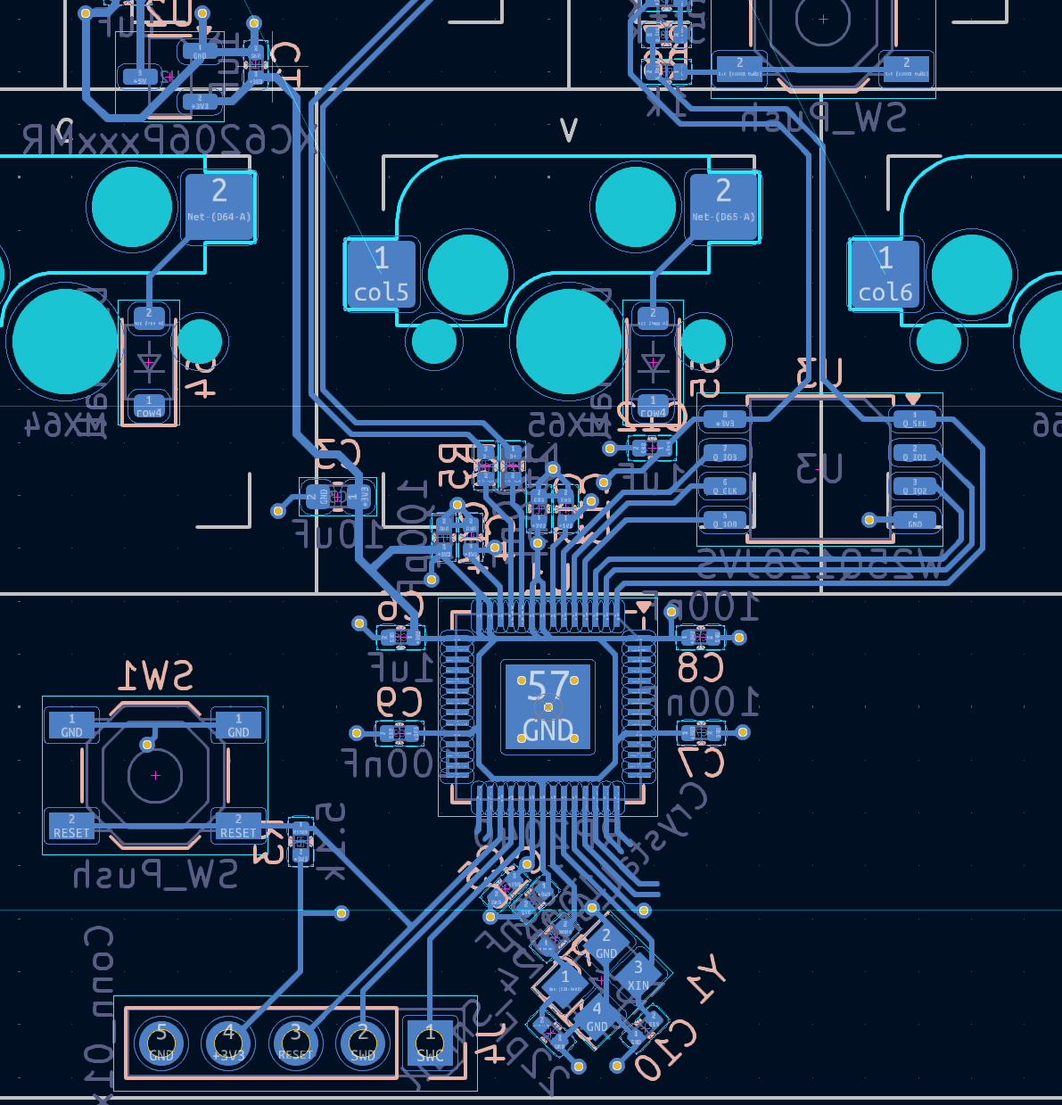
Again, there are several design flaws, especially with the routing, but I fixed the major errors highlighted by the DRC. Open pins will be filled by the switch matrix when they are wired. I had to redo the routing several times in order to get traces to fit together, so this was the best I could for the first draft. I hope to fix most of the design errors in the future when I optimize the design and do rigorous research into proper PCB design practice.
Successes and Failures
This project was certainly a learning experience. I made several errors routing components together (such as 90 degree traces, incorrect trace width, wrong differential pair gap, etc.), but I was able to learn WHY they were wrong and put effort into preventing those mistakes. One major issue that I currently have with this design is that the trace widths are inconsistent and the MCU unit is too far from the USB connector. There are also issues with diode placement for the key witches. One roadblock early on was that I realized that I used an outdated micro-controller with not enough IO pins, so I had to start all over again with a new unit. In the future, I hope to upgrade the RP2040 to the STM32 as the STM32 has better IO, extra built-in circuitry, and generally is easier to code firmware. Another roadblock was trying to fit all the traces in a compact way, which took a lot of playing around with the positioning/software. The most frustrating part was trying to shape the traces in the way I wanted, but due to constraints, it ended up being quite finicky.
There were some successes however. I was pleased with the layout I ended up with as it has all the keys I wanted while having extra space in the top right for peripherals if I wanted to add them. I also became more familiar with the KiCAD shortcuts and settings to help with future problem solving and general design efficiency. While the project was frustrating at times, the knowledge I gained from the tutorials and actually practicing PCB tasks was certainly worth it. I also learned a little bit about general circuit design: the importance of decoupling capacitors, how voltage regulators worked, and the application of diodes. I was familiar with schematic work prior to this project, but now I had the chance to use the PCB editor and learn how to use that.
Skills Gained
Here are some the skills I would say I gained from this project:
- PCB Design (rules, shortcuts, tricks, etc.)
- KiCAD software use
- Circuit Design
- Debugging and Troubleshooting Circuits
- Schematic Documentation
In summary, I learned the very basics of PCB design along with using GitHub to do version control and documentation.
Final Thoughts and Future Plans
This project certainly is worth my time and effort as I am learning an industry skill of PCB design. Although at times frustrating, I was able to overcome obstacles posed by design errors and make solid progress. This was likely not the best design project to learn the fundamentals of PCB design, but I felt I was able to learn from my mistakes much more effectively than if I did a more simple project.
The main technical thing I got out of this project was that a schematic is living document because anything could change at anytime. I also learned the value of doing extensive research and the importance of patience, especially when designing boards with small, sensitive components. I did not know how much effort went into designing PCBs until I had to redo my design several times to get everything to fit together. Despite all the shortcomings and frustrations, I love what this project has taught me and has definitely gotten me more invested in circuit technology and semiconductors. I am looking forward to potentially applying these skills to my Marine Robotics Club as well. This is still ongoing and there still a lot to learn, so I can not wait to make more progress on this keyboard.
Since I have a lot left to go, here is a list of future goals I have for this project:
- Optimize routing and trace width calculations
- Change to a 4-layer PCB to simply routing
- Change the MCU from a RP2040 to a STM32 based chip
- Bring the MCU loop system much closer to the USB 2.0 receptacle
- Adjust the positioning of each diode for the switches
- Mounting holes positioning
- Silkscreen design
- Simulate and check for general design errors based on standard PCB design practices (impedance issues, noise, frequency problems, etc.)
As for much later in the future:
- Add peripherals such as a rotary encoder (volume control), LED screen, solenoid, etc.
- Design a case and switch plate
LED Peripheral for DE-10 Standard | Spring 2025
Problem
The DE-10 Standard Board layout labeled. Credit: RocketBoards Documentation
In teams of 5, we had to make sure the peripheral was easy to use, had a simple API, and was compatible with a simple computer’s ISA (made by the professors). We were encouraged to either create the peripheral with block diagrams or through VHDL, a hardware description language, using Intel’s Quartus Prime to organize the design hierarchy. The professor gave us the barebone simple computer files (SCOMP), and we were supposed to integrate the peripheral within the existing system. Along with designing the actual peripheral, we had to create a solution proposal, log our progress through logbooks, and give a final demonstration with a custom made assembly program (following a given ISA). We had approximately 4-5 weeks to complete the peripheral, demonstration, and the other proposal assignments. While it is impossible to explain every detail of how SCOMP works in a concise matter, here is the general architecture of SCOMP (16-bit, 4 registers with RAM):
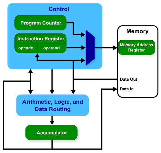
The general architectural overview of the SCOMP processor along with its interface with memory. Credit: ECE 2031 Lab Manual
Solution
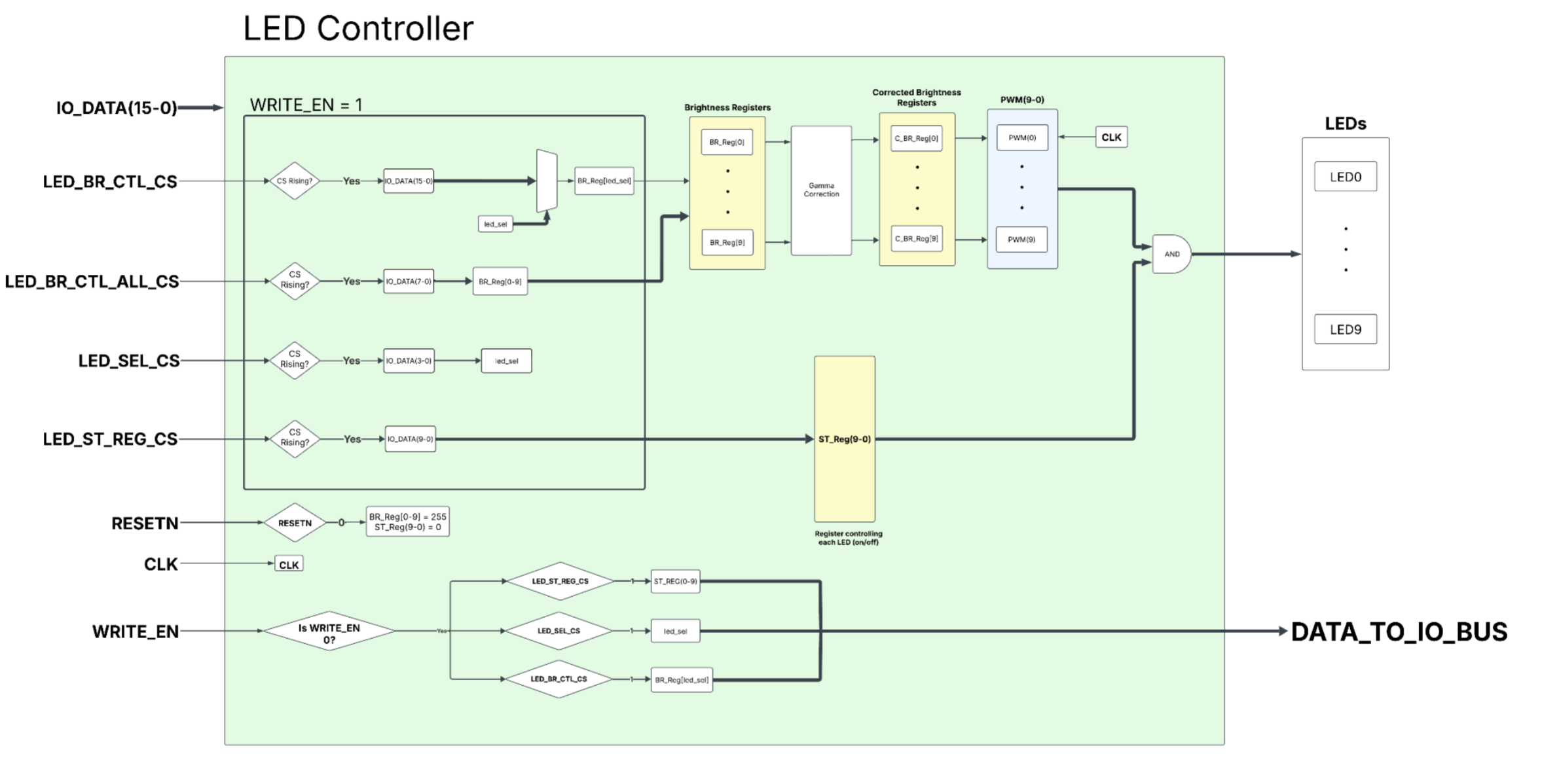
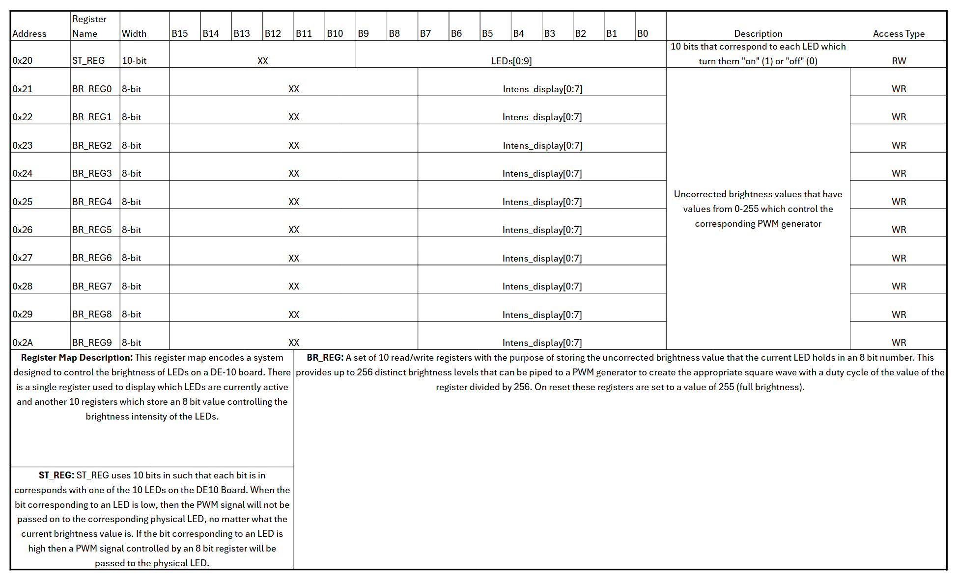
We immediately started brainstorming ideas. At first, we wanted to use the LEDs to have brightness control (through PWM generation), checkpoint tracker (a specific function that allows the user to track checkpoints in their assembly code), and a loop counter, but we realized that implementing all those functionalities would be impossible to do in a month. At the end of the brainstorming process, we decided to prioritize brightness control. To summarize our API, based on the address number the programmer uses, they can control the brightness of individual or every LED on the DE-10 by inputting a standard 0-255 value to the peripheral address(es). Along with that, using a 10-bit bit mask, the programmer could toggle each LED on or off. As a last minute functionality, we also had a read function where the programmer could store a value into the LEDs and read from them whenever they choose. We felt that these four functionalities fulfilled the design challenge and was relatively easy/useful for a SCOMP programmer. I worked on coding the PWM generator (to produce the proper signal for corresponding brightness based on input value) and a gamma correction function to adjust incoming brightness value to human perception of brightness in VHDL, both of which worked properly with slight tweaks to the input clock signal.
Below is a rough diagram of our LED Peripheral architecture:
Along with the diagram, here is a register map that explains the function of each register and address:
Results
In the end, we managed to achieve everything we had decided upon during brainstorming. We could control each LED brightness with around 95% accuracy on the 0-255 scale, as well as a working bit-mask and read functionality to complete our API. The PWM generation worked as expected, as brightness with LEDs is dictated by the high-low cycle of the input signal, and we were able to set the brightness to any value between 0 and 255. To demonstrate all of these functionalities, we made a loading bar animation where each LED slowly increased to max brightness one by one in order. We also did a read functionality at the end of the animation to display the value held in the LEDs on the DE-10’s HEX displays. Unfortunately, I lost the live demo video, but I have attached our supplementary demo presentation along with our original design proposal presentation.